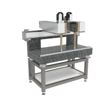
DE
EN
Toggle navigation
Serienentwicklung
Serienentwicklung
Beratung
Entwicklung
Prototypen
Fertigung
Montage
Test und Messung
Inbetriebnahme
Sicherheit
Dokumentation
Glossar
Anwendungen
Anwendungen
Medizin und Biotechnologie
Laborautomation
Labormikroskopie
Bildgebende Verfahren
XYZ Positioniersysteme
Halbleiter
Halbleiter
Standard, Elektronenstrahl, EUV Lithografie
Wafer und Chip Inspektion
XYZ Positioinersysteme
Vakuum
Messtechnik
Messtechnik
Fahrdrahtmessung
Laser und Röntgen
Astronomie und Raumfahrt
Positioniersysteme
Positioniersysteme
OEM-Positioniersysteme
Serienbaugruppen
Additive Fertigung | 3D Druck
Labor | Analytik
Inspektion | Mikroskopie
Justage | Montage | Test
Panoptikum
Referenzen
Mehrachssysteme
Mehrachssysteme
Gantries
Portale
Industrietische
Labortische
Kompakte Mehrachssysteme
Vakuum
Vakuum
Vakuum Lineartische
Vakuum Kreuztische
Vakuum Drehtische
Vakuum Hubtische
Vakuum Mehrachssysteme
Vakuum Kompakte Mehrachssysteme
Standardsysteme
Standardsysteme
Linearachsen
Lineartische
Mikrotische
Kreuztische
Drehtische
Hubtische
Controller
Gewindetriebe
Downloads
Unternehmen
Unternehmen
Steinmeyer Firmengruppe
Steinmeyer Mechatronik GmbH
Presse & Innovationen
Historie
Historie
Zeitreise Innovationen
Zeitreise zurück in den Alltag
Teleskope & Observatorien
Zertifikate
Karriere
Kontakt
Kontakt
Kontakt
Anfrageformular
Webmeeting
Fernzugriff und FTP-Zugang
Service und Reparatur
Technischer Support
Internationale Vertretungen
ALLE SYSTEME
STANDARD
TEXT
PDF
OEM-Positioniersysteme
Safety Laser Shutter for extreme laser beams up to 2 kW
… systems for medical and analytical equipment,
semiconductor
indusy, aircraft insuments, surface...
EUV polarization filter for miniaturization in
semiconduc...
…EUV polarization filter for miniaturization in
semiconductor
lithography | Positioning system for...
Sample manipulator for precise mass spectrometer,...
… of the precision of circuits in the
semiconductor
indusyExplosives detection on clothing and...
XYZ Phi inspection system suitable for 12 inch wafers,...
… can be used for various test and inspection processes in
semiconductor
and eleconics manufacturing...
XYZ positioning system for inspection & metrology by...
… options Ideal base for inspection systems in
semiconductor
or optics manufacturingVery large...
X Phi positioning system for inspection of wafers,...
… system for clean rooms Ideal for inspection tasks in
semiconductor
technology, biotechnology and...
9-axis microscopy station for high-resolution, automated...
… high-precision 3D processes in medicine, biotechnology and
semiconductor
technologyUla-fine...
2-XYZ-Phi System mit Nanometerstabilität zur Micromontage...
… von Herzschrittmachern, Kameras, Insulinpumpen, Packaging
Semiconductor
, innovative...
Mehrachssysteme
9-axis positioning system with travels up to 100 mm | XYZ...
… high-precision 3D processes in medicine, biotechnology and
semiconductor
technologyUla-fine...
X Phi system for the positioning of optical lenses,...
… mapping, surface suctures, laboratory application,
semiconductor
inspection, optical inspection...
XZ System for Laboratory and Wafer Inspection | Ball...
… assurance, 3-axis sensor measurement, wafer inspection,
semiconductor
quality insurance -...
MP210-3
… axis manipulator with large aperture. Manly used in
semiconductor
inspection and for manipulating...
MP200-5
… of components, roundness measuring equipment,
semiconductor
inspection, optical centering systems,...
Vakuum
LA97
… precision scanning applications, micro assembly,
semiconductor
technology in ula-high vacuum and...
LA92
… and fast scanning applications, micro assembly,
semiconductor
technology in ula-high vacuum,...
MT105
… to position higher loads. Fields of application
Semiconductor
technology in ula-high vacuum...
LA170
… of imaging systems, microscopy, analysis of samples,
semiconductor
inspection, quality assurance...
LA80
… in ula-high vacuum under exeme ulaviolet radiation,
semiconductor
fabrication, beam shaping for...
LT300
… in the nanometer range. Fields of application
Semiconductor
technology in ula-high vacuum and...
KDT105
… positioning for laboratory applications, microscopy and
semiconductor
technology, research in...
KDT310
… positioning for laboratory applications, microscopy and
semiconductor
technology, research in...
DT155
… research, materials analysis, wafer inspection,
semiconductor
quality conol,
semiconductor
...
DT65
… research, materials analysis, wafer inspection,
semiconductor
quality conol,
semiconductor
...
MP53-3-PM
… space for laboratory applications, microscopy and
semiconductor
technology, research in ula-high...
MP105-3
… small spaces for laboratory applications, microscopy and
semiconductor
technology, research in...
Standardsysteme
LA340-EDLM
… laser machining, photonics, precision scanning,
semiconductor
or flat panel display manufacturing ...
PLT320-SM
… in indusial environments including laser engineering,
semiconductor
technology and special-purpose...
PMT160-EDLM
… acceleration - for example, in laser technology or the
semiconductor
indusy. Linearencoder...
PLT165-DLM
… is required - such as, for example, lacer machining,
semiconductor
technology or measurement...
PLT240-AC
… environments. Whether it is used in laser engineering,
semiconductor
technology or special-purpose...
MT53-PM
… in research and development applications or in the
semiconductor
indusy. Linearencoder Piezo Motor...
KDT235-DC
… meology, autofocus systems, biotechnology,
semiconductor
testing DC-Motor - Kreuztische
KDT310-DC
… meology, autofocus systems, biotechnology,
semiconductor
testing DC-Motor - Kreuztische
KDT180-NM
… interferomey, meology, autofocus systems, biotechnology,
semiconductor
testing, research,...
KDT180-DC
… assembly, optics positioning, sample positioning,
semiconductor
inspection, measurement systems,...
KT180-DC
… assembly, optics positioning, sample positioning,
semiconductor
inspection, measurement systems,...
KT180-SM
… assembly, optics positioning, sample positioning,
semiconductor
inspection, measurement systems, ...
KT600-EDLM
… Fast scanning applications and dynamic web avel e.g.
semiconductor
inspection, measuring...
KDT600-EDLM
… Fast scanning applications and dynamic web avel e.g.
semiconductor
inspection, measuring...
KT500-EDLM
… Fast scanning applications and dynamic web avel e.g.
semiconductor
inspection, measuring...
KT470-DC
… scanning applications and dynamic web avel e.g.
semiconductor
inspection, measuring systems,...
KT470-SM
… scanning applications and dynamic web avel e.g.
semiconductor
inspection, measuring systems,...
KDT310-SM
… meology, autofocus systems, biotechnology,
semiconductor
testing Schrittmotor - Kreuztische
KDT180-SM
… assembly, optics positioning, sample positioning,
semiconductor
inspection, measurement systems,...
KDT180-PM
… interferomey, meology, autofocus systems, biotechnology,
semiconductor
testing, research,...
Suche
Application Areas
… more [Translate to English:] Teil 2
Semiconductor
Ever smaller chips with...
www.steinmeyer-mechatronik.de
Careers
… In the sectors of laser technology, medical technology,
semiconductor
technology and measurement...
History
… has partners in various industries. These include the
semiconductor
-, laser-, and optical...
Semiconductor
Technology
… to your application - from test labs to automated
semiconductor
factories up to ISO 14644-1 up to...
Unternehmen
Innovations time line
… first cleanroom system for high-precision motion tasks in
semiconductor
technology with air...